- 您现在的位置:买卖IC网 > Sheet目录466 > IXTY08N50D2 (IXYS)MOSFET N-CH 500V 800MA DPAK
IXTY08N50D2
IXTA08N50D2
IXTP08N50D2
Symbol Test Conditions
(T J = 25 ° C, Unless Otherwise Specified)
Characteristic Values
Min. Typ. Max.
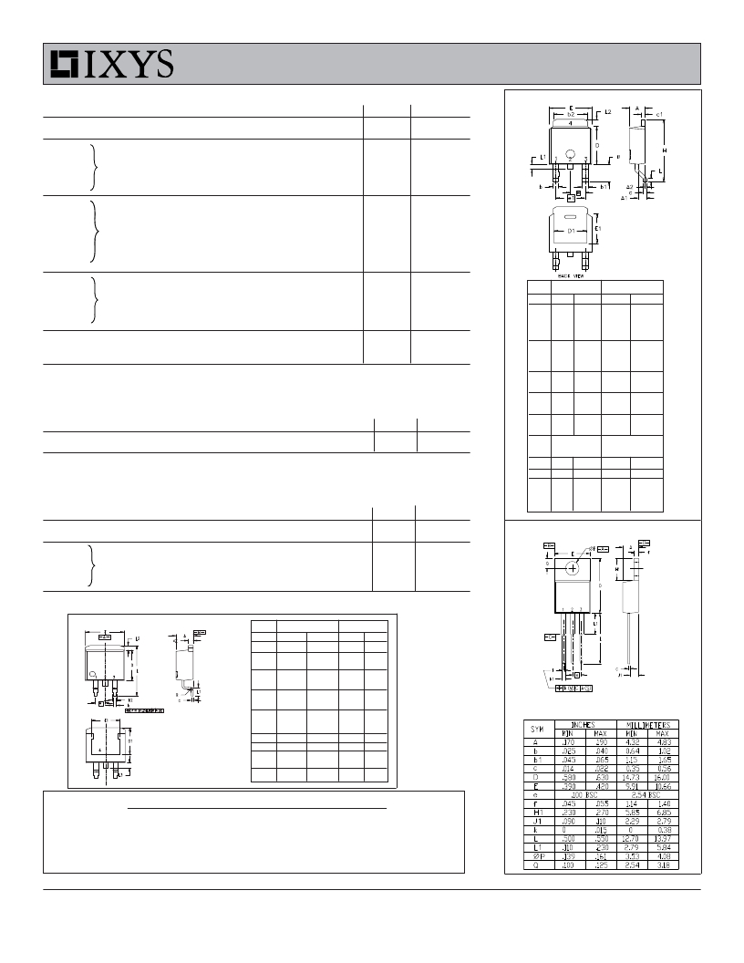
TO-252 AA (IXTY) Outline
g fs
C iss
C oss
C rss
V DS = 30V, I D = 400mA, Note 1
V GS = -10V, V DS = 25V, f = 1MHz
340
570
312
35
11
mS
pF
pF
pF
t d(on)
t r
t d(off)
t f
Resistive Switching Times
V GS = ± 5V, V DS = 250V, I D = 400mA
R G = 10 Ω (External)
28
54
35
52
ns
ns
ns
ns
1.
2.
3.
4.
Gate
Drain
Source
Drain
Bottom Side
Q g(on)
12.7
nC
Dim.
Millimeter
Inches
Q gs
Q gd
V GS = 5V, V DS = 250V, I D = 400mA
1.2
7.3
nC
nC
A
A1
Min. Max.
2.19 2.38
0.89 1.14
Min. Max.
0.086 0.094
0.035 0.045
R thJC
R thCS
TO-220
0.50
2.08 ° C/W
° C/W
A2
b
b1
b2
0
0.64
0.76
5.21
0.13
0.89
1.14
5.46
0
0.025
0.030
0.205
0.005
0.035
0.045
0.215
c
0.46
0.58
0.018
0.023
Safe-Operating-Area Specification
Characteristic Values
c1
D
D1
0.46
5.97
4.32
0.58
6.22
5.21
0.018
0.235
0.170
0.023
0.245
0.205
Symbol
Test Conditions
Min. Typ. Max.
E
E1
6.35
4.32
6.73
5.21
0.250
0.170
0.265
0.205
SOA
V DS = 400V, I D = 90mA, T C = 75 ° C, Tp = 5s
36
W
e
e1
2.28 BSC
4.57 BSC
0.090 BSC
0.180 BSC
H
L
9.40 10.42
0.51 1.02
0.370
0.020
0.410
0.040
Source-Drain Diode
Symbol Test Conditions
(T J = 25 ° C, Unless Otherwise Specified)
Characteristic Values
Min. Typ. Max.
L1
L2
L3
0.64
0.89
2.54
1.02
1.27
2.92
0.025
0.035
0.100
0.040
0.050
0.115
V SD
t rr
I RM
Q RM
I F = 800mA, V GS = -10V, Note 1
I F = 800mA, -di/dt = 100A/ μ s
V R = 100V, V GS = -10V
0.8
400
5.2
1.04
1.3
V
ns
A
μ C
TO-220 (IXTP) Outline
Note 1. Pulse test, t ≤ 300 μ s, duty cycle, d ≤ 2%.
TO-263 (IXTA) Outline
Dim.
Millimeter
Min. Max.
Inches
Min. Max.
A
b
b2
c
c2
4.06
0.51
1.14
0.40
1.14
4.83
0.99
1.40
0.74
1.40
.160
.020
.045
.016
.045
.190
.039
.055
.029
.055
1.
2.
3.
4.
Gate
Drain
Source
Drain
D
D1
E
E1
e
L
L1
L2
8.64
8.00
9.65
6.22
2.54
14.61
2.29
1.02
9.65
8.89
10.41
8.13
BSC
15.88
2.79
1.40
.340
.280
.380
.270
.100
.575
.090
.040
.380
.320
.405
.320
BSC
.625
.110
.055
Pins:
1 - Gate
3 - Source
2 - Drain
4 - Drain
L3
1.27
1.78
.050
.070
PRELIMINARY TECHNICAL INFORMATION
The product presented herein is under development. The Technical Specifications offered are derived
from data gathered during objective characterizations of preliminary engineering lots; but also may yet
contain some information supplied during a pre-production design evaluation. IXYS reserves the right
to change limits, test conditions, and dimensions without notice.
IXYS Reserves the Right to Change Limits, Test Conditions, and Dimensions.
IXYS MOSFETs and IGBTs are covered
4,835,592
4,931,844
5,049,961
5,237,481
6,162,665
6,404,065 B1
6,683,344 6,727,585 7,005,734 B2
7,157,338B2
by one or more of the following U.S. patents: 4,850,072
5,017,508
5,063,307
5,381,025
6,259,123 B1
6,534,343
6,710,405 B2 6,759,692 7,063,975 B2
4,881,106
5,034,796
5,187,117
5,486,715
6,306,728 B1
6,583,505
6,710,463
6,771,478 B2 7,071,537
发布紧急采购,3分钟左右您将得到回复。
相关PDF资料
IXTY1N80P
MOSFET N-CH 800V 1A TO-252
IXTY1N80
MOSFET N-CH 800V 750MA TO-252AA
IXTY1R6N100D2
MOSFET N-CH 1000V 1.6A DPAK
IXTY2N60P
MOSFET N-CH 600V 2A D-PAK
IXTY4N60P
MOSFET N-CH TO-252
IXTY55N075T
MOSFET N-CH 75V 55A TO-252
IXTZ550N055T2
MOSFET N-CH 55V 550A DE475
IXUC160N075
MOSFET N-CH 75V 160A ISOPLUS220
相关代理商/技术参数
IXTY10P15T
功能描述:MOSFET TrenchP Power MOSFET RoHS:否 制造商:STMicroelectronics 晶体管极性:N-Channel 汲极/源极击穿电压:650 V 闸/源击穿电压:25 V 漏极连续电流:130 A 电阻汲极/源极 RDS(导通):0.014 Ohms 配置:Single 最大工作温度: 安装风格:Through Hole 封装 / 箱体:Max247 封装:Tube
IXTY12N06T
功能描述:MOSFET 12 Amps 6V RoHS:否 制造商:STMicroelectronics 晶体管极性:N-Channel 汲极/源极击穿电压:650 V 闸/源击穿电压:25 V 漏极连续电流:130 A 电阻汲极/源极 RDS(导通):0.014 Ohms 配置:Single 最大工作温度: 安装风格:Through Hole 封装 / 箱体:Max247 封装:Tube
IXTY12N06TTRL
制造商:IXYS Corporation 功能描述:MOSFET N-CH 60V 12A TO-252
IXTY15N20T
功能描述:MOSFET 15 Amps 200V 180 Rds RoHS:否 制造商:STMicroelectronics 晶体管极性:N-Channel 汲极/源极击穿电压:650 V 闸/源击穿电压:25 V 漏极连续电流:130 A 电阻汲极/源极 RDS(导通):0.014 Ohms 配置:Single 最大工作温度: 安装风格:Through Hole 封装 / 箱体:Max247 封装:Tube
IXTY15P15T
功能描述:MOSFET TrenchP Power MOSFET RoHS:否 制造商:STMicroelectronics 晶体管极性:N-Channel 汲极/源极击穿电压:650 V 闸/源击穿电压:25 V 漏极连续电流:130 A 电阻汲极/源极 RDS(导通):0.014 Ohms 配置:Single 最大工作温度: 安装风格:Through Hole 封装 / 箱体:Max247 封装:Tube
IXTY18P10T
制造商:IXYS Corporation 功能描述:MOSFET P-CH 100V 18A TO-252
IXTY1N100P
功能描述:MOSFET 1 Amps 1000V 14 Rds RoHS:否 制造商:STMicroelectronics 晶体管极性:N-Channel 汲极/源极击穿电压:650 V 闸/源击穿电压:25 V 漏极连续电流:130 A 电阻汲极/源极 RDS(导通):0.014 Ohms 配置:Single 最大工作温度: 安装风格:Through Hole 封装 / 箱体:Max247 封装:Tube
IXTY1N120P
功能描述:MOSFET N-CH 1200V 1A TO-252 RoHS:是 类别:分离式半导体产品 >> FET - 单 系列:- 标准包装:1,000 系列:MESH OVERLAY™ FET 型:MOSFET N 通道,金属氧化物 FET 特点:逻辑电平门 漏极至源极电压(Vdss):200V 电流 - 连续漏极(Id) @ 25° C:18A 开态Rds(最大)@ Id, Vgs @ 25° C:180 毫欧 @ 9A,10V Id 时的 Vgs(th)(最大):4V @ 250µA 闸电荷(Qg) @ Vgs:72nC @ 10V 输入电容 (Ciss) @ Vds:1560pF @ 25V 功率 - 最大:40W 安装类型:通孔 封装/外壳:TO-220-3 整包 供应商设备封装:TO-220FP 包装:管件
